How our Nanosensors are made
Until now, MEMS sensors are all created using expensive proprietary processes to build the MEMS sensor structure on the top of a CMOS wafer. Each design of MEMS sensor needs a unique process to make the structure that takes 5-7 years to perfect and there are no economies of scale or ability to rapidly ramp production apart from duplicating the production line.
Nanusens creates nanoscale sensor structures inside the CMOS layers using standard CMOS processes within the same production flow as making the control electronics on the same chip. This innovative approach reduces the size and cost as it benefits from the vast economies of scale of using giant CMOS fabs. The resulting single chip solution has a packaged size of only 0.5 mm3.
We use 0.18-micron CMOS technology as it is a well-established, high volume technology used by most fabs giving us the freedom to use any fab. This is important as it means that we can rapidly ramp production to whatever volumes are required. We can also benefit from lower costs simply by moving to smaller CMOS process nodes.
The Inter Metal Dielectric (IMD) is etched away through the pad openings in the passivation layer using vapour HF (vHF) to create the nanosensor structures. The holes are then sealed and the chip packaged as necessary. As only standard CMOS processes with minimal post-processing are used, they can have high yields similar to CMOS devices. This also means that the production is fab-independent.


How our Sensor works
This scanning electron microscope picture show the structure of a Nanusens motion sensor that detects movement in one plane – up and down in this illustration. The design consists of a load mass in the middle supported off of four rectangular pillars via four springs. The interleaved ‘fingers’ on the left- and right-hand side move relative to one another as the load mass moves. This movement is detected by the change in the capacitance between the fingers.
Multiple Sensors on one Chip
We will soon be making combination solutions with several nanosensors on the same chip. This is very easy for us to do as all our sensors use the same standard CMOS techniques to make them. What’s really exciting is that the additional sensor structures are all about the same tiny size so that there is only a tiny increase in the overall chip size as we add more sensor structures. The control electronics are mainly shared so again hardly any size increase as the number of sensors increases from this aspect. Now designers can add sensors for improved functionality and device awareness without having to sacrifice valuable space.
In addition, a single package solution with multiple sensors needs far less PCB real estate than a set of individually packaged MEMS sensors.


Rugged
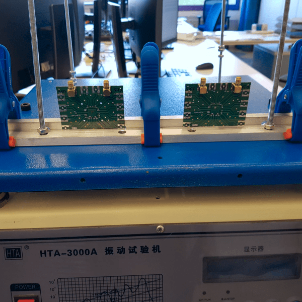
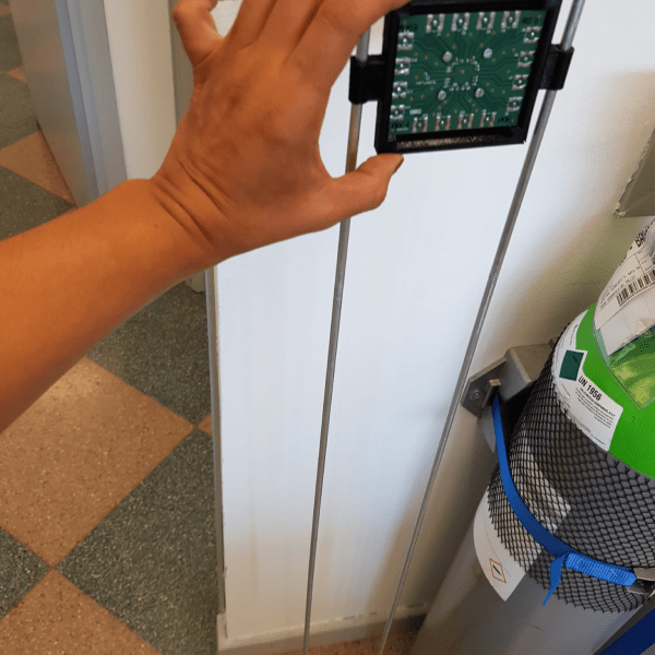
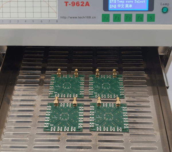
Importantly for a sensor in a device that is likely to be dropped, our NEMS designs are more robust and reliable than MEMS designs. This is because, when dropped, the large load mass of a MEMS hits another part of the MEMS and sticks due to Van der Waals or Casimir forces creating reliability issues for MEMS. By contrast, there is less mass in a small, light NEMS load mass so these forces have less of an effect. The NEMS device is thus much less likely to be affected by impacts, making it more rugged and reliable.